Chemical reactions are used to achieve the fine
structures present in current integrated circuits. This
electron micrograph shows a transistor in a "cell" of a
random access memory chip.
|
Almost every aspect of our lives—at work, at home, and in recreation-has been affected by the information revolution. Today, information is collected, processed, displayed, stored, retrieved, and transmitted by an array of powerful technologies that rely on electronic microcircuits, light wave communication systems, magnetic and optical data storage and recording, and electrical interconnections. Materials and devices for these technologies, along with photovoltaic materials and devices, are manufactured by sophisticated chemical processes. The United States is now engaged in fierce international competition to achieve and maintain leadership in the design and manufacture of these materials and devices. The economic stakes are large; national productivity and security interests dictate that we make the strongest possible effort to stay ahead in processing science and technology for this area. In the manufacturing of components for in- formation and photovoltaic systems, there has been a long-term trend away from mechanical production and toward production by chemical processes. Chemists and chemical engineers have become increasingly involved in several areas of research and process development. Worldwide, however, many high-technology industries, such as microelectronics, still have surprisingly little strength in chemical processing and engineering. The United States has a particular advantage over its international competitors in that its chemical engineering research community leads the world in size and sophistication. The United States is in a position to exploit its strong competence in chemical processing to regain leadership in areas where the initiative in manufacturing technology has passed to Japan and to maintain or increase leadership in areas of U.S. technological strength. Chemical engineering contributes to research on information and photovoltaic materials and devices in a variety of ways. As a discipline it is involved in the large scale synthesis of materials, the design and optimization of reaction and deposition processes, the treatment of waste streams arising from materials processing, and process integration and automation associated with packaging and assembly. The array of materials processed by chemical engineers in this industry is far too large to mention. Elements from almost every column in the periodic table have been used to make insulators, semiconductors, conductors, waveguides, optical transmitters and sensors, and protective coatings. Within the microelectronics industry, two classes of materials have received a lot of attention since the invention of the transistor. These are called II-VI (two-six) and III-V (three-five) compounds, after the columns in the periodic table containing the elements of interest. The II-VI compounds may contain group II metals such as beryllium, magnesium, or barium, and group VI nonmetals such as oxygen or sulfur. Different combinations of the II-VI elements are used to make non-electrically conducting films such as magnesium oxide (MgO), which may be used as substrates in disk drives or high temperature superconductors. The III-V compounds may contain group III metals such as gallium, aluminum, or indium, and group V nonmetals such as nitrogen, phosphorous, arsenic, or antimony. Different combinations of III-V elements are used to make binary, ternary, and quaternary alloys that have optoelectronic properties, that is, they emit light when electrical current is passed through them. We know these as solid state lasers, among other things, such as those found in barcode scanners at supermarket checkouts. An exciting component of working in these industries is the direct interaction with other disciplines. Chemical engineers have had to become able to communicate across disciplinary lines, as the technologies discussed in this section involve solid-state physics and chemistry, electrical engineering, and materials science. Electronic, photonic, and recording materials and devices may seem to be an exceedingly diverse class of materials, but they have many characteristics in common: their products are high in value; they require relatively small amounts of energy or materials to manufacture; they have short commercial life cycles; and their markets are fiercely competitive—consequently, these products experience rapid price erosion. The manufacturing methods used to produce integrated circuits, interconnections, optical fibers, recording media, and photovoltaics also share characteristics. All involve a sequence of individual, complex steps, most of which entail the chemical modification or synthesis of materials. The individual steps are designed as discrete unit or batch operations and, to date, there has been little effort to integrate the overall manufacturing process. Chemical engineers can play a significant role in improving manufacturing processes and techniques, and investments in chemical processing science and engineering research represent a potentially high-leverage approach to enhancing our competitive position. |
|
Before the invention of the transistor in 1948, the electronics industry was based on vacuum tube technology, and most electronic gear was assembled on a metal chassis with mechanical attachment, soldering, and hand wiring. All the components of pretransistor electronic products—vacuum tubes, capacitors, inductors, and resistors—were manufactured by mechanical processes. A rapid evolution occurred in the electronics industry after the invention of the transistor and the monolithic intelrated circuit:
The importance and sophistication of current chemical manufacturing processes for electronic, photonic, and recording materials ant devices are not widely appreciated. A more detailed description serves to highlight their central role in these technologies. Microcircuits Microcircuitry has been made possible by our ability to use chemical reactions and processes to fabricate millions of electronic components or elements simultaneously on a single substrate, usually silicon. For example, the 128-million-bit dynamic random access memory (DRAM) device shown below contains 130 million transistors and over 100 million capacitors, with some chemically etched features on the chip being as small as 0.25 microns (0.00001 inch). This stunning achievement is just one step in a long-term trend toward the design and production of integrated circuits of increasing complexity and capability. There is still considerable room for further increases in component density in silicon-based microelectronics, not to mention possible advances in component density that would result from alternative methods of storing and transferring information (e.g., three-dimensional circuits, quantum junctions, and optical devices). |
|
Chemical reactions are used to achieve the fine
structures present in current integrated circuits. This
electron micrograph shows a transistor in a "cell" of a
random access memory chip.
|
|
Chemical reactions and processes in the manufacture of microcircuits begin with the basic material for integrated circuits, high-purity polycrystalline silicon (for each trillion atoms, less than 100 are elements other than silicon). This ultrapure silicon is produced from 98% pure silicon by the following steps: (1) reaction at high temperature with hydrogen chloride (HCl) to form a complex chemical mixture containing trichlorosilane (SiHCl3); (2) separation and purification of trichlorosilane; and (3) reduction of ultrapure trichlorosilane to polycrystalline silicon by reaction with hydrogen at 1,100-1,200 ºC. To prepare single-crystal silicon ingots (also known as boules, pronounced "bools") suitable for use as materials in semiconductors, polycrystalline silicon is melted in a crucible at 1,400-1,500 ºC under an inert atmosphere, usually pure argon. Very small amounts of dopants—compounds of phosphorous, arsenic, or boron—are the added to the melt to achieve the desired electrical properties of the finished single-crystal wafers. A tiny seed crystal of silicon with the proper crystalline orientation is inserted into the melt and slowly rotated and withdrawn at a precisely controlled rate, forming a large cylindrical single crystal 6 inches (14 cm) in diameter and about as tall as an adult human being (1.8 m) with the desired crystalline orientation and composition. Crystal growth kinetics, heat and mas transfer relationships, and chemical reactions all play important roles in this process of controller growth. The resulting single crystal ingots are sawed into wafers that are polished to a flatness in the range of from 1 to 10 microns (0.00004-0.0004 inch).
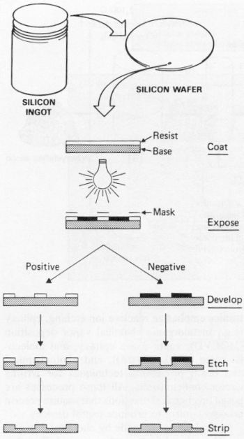
The next steps in device fabrication are the sequential deposition and patterning of thin dielectric (insulating) and conducting films, illustrated in the figure below. The polished silicon wafer is first oxidized in a furnace at 1,000–1,200 ºC. The resulting silicon dioxide (SiO2) film is a few hundred nanometers thick and extremely uniform (a nanometer is one-thousandth of a micron, and a micron is 0.00004 inch). The wafer is then coated with a photosensitive polymeric material, call a resist, and is exposed to light through the appropriate photomask. The purpose of the photolithographic process is to transfer the mask pattern to the thin silicon dioxide film on the wafer surface. The exposed polymer film is developed with a solvent that removes unwanted portions, and the resulting pattern serves as a mask for chemically etching the pattern into the silicon dioxide layer. |
||
|
A number of sequentual chemical steps are used
to take the pure silicon wafer and pattern it so that
integrated circuits can be laid down.
|
|
The resist is then removed with an oxidizing agent such as sulfuric acid-hydrogen peroxide (H2SO4-H2O2) mixture, and the wafer is chemicall cleaned and ready for other steps in the fabrication process. The patterned wafer might next be placed in a diffusion furnace, where a first doping step is performed to deposit phosphorous or boron into the holes in the oxide layer. A new oxide film can then be grown and the photoresist process repeated. As many as 15 layers of conductor, semiconductor, and dielectric materials are deposited, etched, and/or doped to build the three-dimensional structure of the microcircuit. |
|
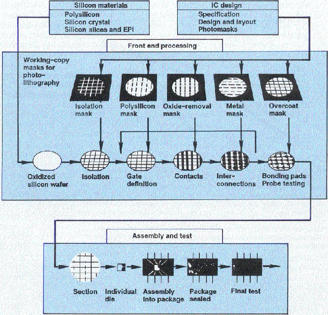
The manufacture of integrated circuits requires
both expertise in electronic design and chemical processing.
Chemical process steps are important to the preparation of
silicon materials, to the steps from oxidation of silicon
wafers through establishment of bonding pads, and to the
final assembly of chips in individual packages. (Click on
image for larger view.)
|
|
Light wave and media devices Other applications for light guides, such as optical fiber sensors and transducers, are receiving a great deal of attention. Image transmission (e.g., endoscopes), energy transmission (e.g., light pipes), and display (e.g., decorative signs) are growing commercial areas. Light wave media and devices include the guiding medium (optical fibers), sending and receiving devices, and associated electronics and circuitry. The transmission of light signals through optical fibers must occur at wavelengths where the absorption of light by the fiber is at a minimum. Typically, for silicon dioxide/germanium dioxide (SiO2/GeO2) glass, the best transmission windows are at 1.3 or 1.5 microns. In other words, the best transmission, and commensurate least losses due to absorbtion occur in this glass fiber when the wavelength of light is either 1.3 microns or 1.5 microns. Optical signal processing for integrated optics and optical computing is still at a relatively early stage but is certain to be an important area for future technological development. The processing involved in making optoelectronic devices is very similar to that used in microcircuit manufacture, but with considerable utilization of the III-V compound semiconductors discussed in the last section, lithium niobate, and a variety of polymeric materials. Developmental manufacturing processes for optoelectronics emphasize reactive ion etching, epitaxy (e.g., metalorganic chemical vapor deposition (MOCVD), vapor-phase epitaxy, and molecular-beam epitaxy (MBE)), and photochemical and beam processing techniques for writing circuit configurations. All these processes are based on chemical reactions that require precise process control to produce useful devices.
Optical fibers are made by chemical processes. The critical feature of an optical fiber that allows it to propagate light down its length is a core of high refractive index surrounded by a cladding of lower index. The higher index core is produced by doping silica with oxides of phosphorus, germanium, and/or aluminum. The cladding is either pure silica or silica doped with fluorides or boron oxide. There are four principal processes that may be used to manufacture the glass body that is drawn into today's optical fiber. "Outside" processes-outside vapor-phase oxidation and vertical axial deposition-produce layered deposits of doped silica by varying the concentration of silicon tetrachloride (SiCI4) and dopants passing through a torch. The resulting "soot" of doped silica is deposited and partially sintered to form a porous silica boule. Next, the boule is sintered to a pore-free glass rod of near-perfect purity and transparancy. "Inside" processes, such as modified chemical vapor deposition (MCVD) and plasma assisted chemical vapor deposition (PACVD), deposit doped silica on the interior surface of a fused silica tube. In MCVD, the oxidation of the halide reactants is initiated by a flame that heats the outside of the tube. In PACVD, the reaction is initiated by a microwave plasma. More than a hundred different layers with different refractive indexes (a function of glass composition) may be deposited by either process before the tube is collapsed to form a glass rod. In current manufacturing plants for glass fiber, the glass rods formed by all the above processes are carried to another facility where they are drawn into a thin fiber and immediately coated with a polymer. The polymer coating is important; it protects the fiber surface from microscopic scratches, which can seriously degrade the glass fiber's strength. Current manufacturing technologies for optical fiber are expensive compared with the low cost of commodity glass. U.S. economic competitiveness in optical technologies would be greatly enhanced if low-cost means were found for producing wave guide-quality silica glass. The manufacture of glass lends itself to a fully integrated and automated (i.e., continuous) process. One can envision a fiber manufacturing plant that moves from purification of chemical reagents to a series of chemical reactions, glass-forming operations, and, finally, fiber-drawing steps. Intermediate products would never be removed from the production line. Sol-gel and related processes are attractive candidates for such a manufacturing technology, which would start with inexpensive ingredients and proceed from a sol to a gel, to a porous silica body, to a dried and sintered glass rod, to drawn and coated fibers. Such a process could reduce the cost of glass fiber by as much as a factor of 10, a step that would greatly increase the scope, availability, and competi- tiveness of light wave technologies. At present the chemical steps involved in sol-gel processes are poorly understood. Methods are being sought to manipulate these processes to produce precisely layered structures in a reliable and reproducible way. Photovoltaics The optoelectronic properties of a III-V material such as GaAs make it particularly promising for this application. The same physical process responsible for converting electrical potential (voltage) into emitted light in GaAs works to turn incident light into electricity. Gallium arsenide cells have achieved high energy efficiencies (in excess of 20 percent) and have been successfully used in systems where there is magnification of the sun's rays, that is, concentrator systems that increase the light flux per unit area. Substantial research is being devoted to improving the conversion efficiency and lowering the cost per kilowatt of such devices. The materials and processes used in the manufacture of photoelectric energy conversion devices are almost identical to those used in manufacturing microelectronic devices and in- tegrated circuits. The photovoltaics industry could expand rapidly if the efficiency of polycrystalline modules could be increased to 15 percent, if these modules could be built with assurance of reliability over a 10- to 20-year period, and if they could be manufactured for $100 or less per square meter (less than $10 per square foot). Solar energy research has been largely directed toward only one of these issues: efficiency. All research aimed at reducing manufacturing costs has been done in industry and has been largely empirical. Almost no fundamental engineering research has been done on either the laboratory scale or the pilot plant scale for cost-effective processes for the production of photoconverters. Superconductors The key to the superconducting properties of these ceramics seems to be the presence of planes of copper and oxygen atoms bonded to one another. The significance of the other atoms in the lattice seems to be to provide a structural framework for the copper and oxygen atoms. Thus, in the superconducting compound YBa2Cu3O (yttrium-barrium-copper-oxide), the substitution of other rare earths for yttrium results in little change in the properties of the material. This general class of high temperature superconducting compounds is often referred to as YBCO, based on the the four elements originally found to show high temperature superconducting behavior. Currently, high temperature superconducting materials are generally produced by standard techniques from the ceramics industry: mixing, grinding, and sintering (heating to just below the melting point). The basic structure of the 95 K (–178 ºC) superconductors is formed at temperatures above 800–900 ºC, and then annealed with oxygen at a temperature below 500 ºC. More needs to be known about the effect of various synthesis conditions on the microstructure found in these materials. Alternative routes to ceramics, such as sol-gel processes, may lead to significant improvements in the production of these materials. For microelectronic applications, various chemical vapor deposition routes to these materials are currently an active area of investigation. In particular, metalorganic chemical vapor deposition (MOCVD) is proving to be a particularly promising route because relatively volatile precursor compounds have been discovered and synthesized by chemists. Chemical engineers have the necessary background for developing this technology as well as finding the optimal procedure for drying, sintering, and calcining the final product. |
||
|
A variety of important chemical engineering research issues dominate the contribution of this profession to the microelectronics, photonics, storage media, and thin film industries. These issues are quite broad and cut across the spectrum of materials, devices, and applications. Process integration is the key challenge in the design of efficient and cost-effective manufacturing processes for electronic, photonic, and recording materials and devices. Except for magnetic tape, these products are often manufactured through a series of individual, isolated steps. To improve process reliabilty and enhance our capabilities, it is crucial that its overall manufacturing methodology be examined and that integrated manufacturing approaches be implemented. Historically, all industries have benefited both economically and in the quality and yield of products by the use of integrated manufacturing methods. As individual process steps become more complex and precise, the final results of manufacturing (e.g., yield, throughput, and reliability) often depend critically on the interactions among the various steps. Thus, it becomes increasingly important to automate and integrate individual process steps into an overall manufacturing process. The concepts of chemical engineering are easily applied in meeting the challenge of process integration, particularly because many of the key process steps involve chemical reactions. For example, in the manufacture of microcircuits, chemical engineers provide mathematical models and control algorithms for the transient and steady-state operation of individual chemical process steps (e.g., lithography, etching, film deposition, diffusion, and oxidation), as well as interactions between process steps and ultimately between processing and the characteristics of the final device. As another example, in microcircuit manufacture, chemical engineers provide needed simulations of the dynamics of material movement through the plant and thus optimize the flow of devices (or wafers) through a fabrication line. The continuous production of photovoltaic devices will require similar studies with even more emphasis on automation. |
|
Closely related to challenges in process integration are those in reactor engineering and design. Chemical engineering contributions to research in this area are critical for the automation of manufacturing processes to achieve higher yields and improved product quality. Processes such as chemical vapor deposition (CVD), epitaxy, plasma-assisted CVD (PACVD), plasma-enhanced etching, reactive sputtering, and oxidation all take place in chemical reactors. At present, processes and reactors are generally developed and refined by trial and error. A basic understanding of fundamental phenomena and reactor design would facilitate process design, control, and reliability. Because all these processes involve reaction kinetics, mass transfer, and fluid flow, chemical engineers bring a rich background to their study and improvement. For example, high-yield, continuous processes for film deposition and packaging are required if photovoltaic devices are to be manufactured at costs that are com- petitive with other energy technologies. New reactors and a better understanding of chemical dynamics in reactors are central to achieving this. An important consideration in reactor design and engineering is the ultraclean storage and transfer of chemicals. This is not a trivial problem; generally, the containers and transfer media are the primary sources of contamination in manufacturing. Methods are needed for storing gases and liquids, for purifying them, and for delivering them to the equipment where they will be used—all the while maintaining impurity levels below 1 part per billion. (Parts per million (ppm), parts per billion (ppb), and parts per trillion (ppt) are common ways of describing impurity levels in systems, whether it's the purity of a silicon wafer of the purity of water in a lake. The phrase "below 1 ppb" means that, for every billion units—atoms, molecules, grams, ounces, whatever—there is less than one unit of foreign material.) This requirement puts severe constraints on the types of materials that can be used in handling chemicals. For example, materials in reactor construction that might be chosen primarily on the basis of safety often cannot be used. Designs are needed that will meet the multiple objectives of high purity, safety, and low cost. The ultimate limit to the size of microelectronic devices is of molecular dimensions. The ability to "tailor" films at the molecular level—to deposit a film and control its properties by altering or forming the structure, atomic layer by atomic layer—opens exciting possibilities for new types of devices and structures. The fabrication of these multilayer, multimaterial structures will require deposition methods such as MBE (molecular beam epitaxy) and MOCVD. Depositing uniform films bv these methods over large dimensions will require reactors with a different design from those currently used, especially for epitaxial growth processes. The challenge is to be able to control the flow of reactants to build layered structures tens of atoms thick (e.g., superlattices). To achieve economic automated processes, the reactor design must allow for the acquisition of detailed real-time information on the surface processes taking place, fed back into an exquisite control system and reagent delivery system. This problem gives rise to an exciting series of basic research topics. This need for ultrapure materials is particularly acute for semiconductor materials and optical fibers. For semiconductor materials, the challenge is to find new, lower cost routes to ultrapure silicon and III-V materials such as gallium arsenide, and to purify other reagents used in the manufacturing process so that they do not introduce particulate contamination or other defects into the device being manufac- tured. For optical fibers, precursor materials of high purity are also needed. For example, the silicon tetrachloride (SiCI4) currently used in optical fiber manufacture must have a total of less than 4 ppm of hydrogen-containing compounds and less than 2 ppb of metal compounds. A generic plant for the production of ultrapure SiCl4 is shown in the figure below. Either impurity will result in strong light absorption in the glass fiber. For magnetic media, the challenge is to separate and purify submicrometer-sized magnetic particles to very exacting size and shape tolerances. A variety of separation research topics bear on these needs, such as generation of improved selectivity in separations by tailoring the chemical and steric (geometric) interactions of separating agents, understanding and exploiting interfacial phenomena in separations, improving the rate and capacity of separations, and finding improved process configurations for separations. These are all research issues central to chemical engineering. |
|
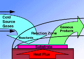
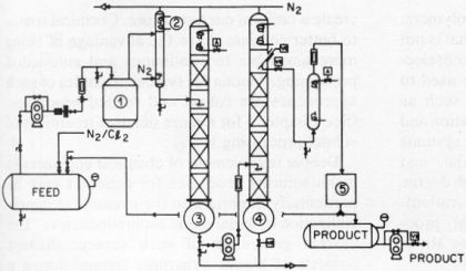
Conceptual diagram of chemical plant for
producing ultrapure silicon tetrachloride, which is used in
the production of optical fibers. The silica feed is passed
through a reactor (1) where chlorination takes place.
Excess hydrochloric acid generated in the reactor is removed
(2) and the stream is passed along to two distillation
columns, or stills, (3,4), where contaminants are removed.
On-line optical sensing (5) is used to monitor final product
purity.
|
|
Polymeric materials For the processing of microcircuits and in- terconnecting devices, improved radiation-sensitive polymers are needed for the formulation of better photoresists. Resists must be highly sensitive to the radiation (that is, the wavelength of light) used for exposure, but not to the microwave radiation used after development for other process steps such as plasma etching. Chemical engineering studies of polymer behavior during development steps are also needed. Details of the dissolution of the exposed (or unexposed) regions of the resist are at present poorly understood. There is a need for fundamental studies and modeling of the formation of a swollen gel layer at the solvent/polymer interface and the subsequent diffusion of polymer chains into solution. Light wave technologies provide a number of special challenges for polymeric materials. Polymer fibers offer the best potential for optical communications in local area network (LAN) applications, because their large core size makes it relatively cheap to attach connectors to them. There is a need for polymer fibers that have low losses and that can transmit the bandwidths needed for LAN applications; the acrylate and methacrylate polymers now under study have poor loss and bandwidth performance. Research on monomer purification, polymerization to precise molecular-size distributions, and well-controlled drawing processes is relevant here. There is also a need for precision plastic molding processes for mass production of optical fiber connectors and splice hardware. A tenfold reduction in the cost of fiber and related devices is necessary to make the utilization of optical fiber and related devices economical for local area networks and the telecommunications loop. Another challenge for polymer research in light wave applications is in the use of active coatings on optical fibers as transducers for sensors. Such coatings may have magnetostrictive or piezoelectric properties. These coatings, or the fiber itself, may also incorporate dyes that would respond to chemicals, light, radiation, or other stimuli to produce transmission loss changes in the fiber. Such systems have enormous potential as sensors that would be ultrasensitive, capable of distributed sensing, able to operate in harsh environments, and unaffected by electromagnetic interference. Specialty fibers such as polarization-maintaining fibers, which have an asymmetric core and can double the bandwidth by transmitting two modes at once, may also play an important role in sensor technology. Techniques for fabricating low-cost optical components such as graded index lenses, microlenses, couplers, splatters, and polarizers are needed to support optical fiber technology. Traditionally, amorphous inorganic materials have been used, but there are tremendous opportunities for innovation with polymers, which offer manufacturing versatility that is not available with glass. For example, photoselective polymerization techniques can be used to make branching wave guide circuits such as splatters and couplers. Photopolymerization and copolymerization of multiple monomer systems have been used to make radial, axial, and spherical graded-index lenses with a high degree of perfection (e.g., freedom from aberration). Large-scale, well-controlled chemical processes will be needed to fabricate these structures. For recording applications, new approaches to high-quality polymeric film substrates are needed. Improved automation and control of thin-film coating are also important. For interconnection and packaging technologies, an important goal is to achieve high-purity molding and dielectric materials. Epoxy-Novolac prepolymers with ionic impurity levels below 20 ppm offer one approach. There is a further need for low-viscosity molding compounds to minimize the development of flow stresses during processing. Continued development of thermally stable polymers with low dielectric constants (such as the polyimides) is also necessary. Advances in our fundamental understanding of polymer chemistry and rheology (flow behavior) are crucial for all these areas. Ceramic materials Deeper involvement of chemical engineers in manufacturing processes for ceramics is particularly important to the eventual commer- cialization of metal oxide superconductors. The current generation of such superconductors consists of planar structures formed during a conventional ceramic synthesis. The ability to precisely control complex phase structure and phase boundaries seems critical. It is by no means clear that the formulations and structures that may produce optimal performance in superconducting ceramics (e.g., room-temperature superconductivity, capacity for high-current density) are accessible by these techniques. Rational synthesis of structured ceramics by chemical processing may be crucial to further improvements in superconducting properties and to efficient large-scale production. |
|
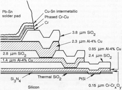
Precise and reproducible deposition of thin films is another area of great importance in the chemical processing of materials and devices for the information age and for protective coating in aeronautics, space, combustion, and other high tech applications. In microelectronic devices, there is a steady trend toward decreasing pattern sizes, and at the beginning of the new millennium the smallest pattern size on a production circuit has now reached 0.25 microns (0.00001 inch); engineers are currently pushing towards 0.1 microns. Although the lithographic tools to print such patterns exist, the exposure step is only one of a number of processes that must be performed sequentially in a mass production environment without creating defects. Precise and uniform deposition of materials as very thin films onto substrates up to 12 inches (30 cm) in diameter must be performed in a reactor, usually at reduced pressure. Particulate defects larger than 0.1 micron must be virtually nonexistent, and as we push to even smaller feature sizes this defect tolerance will need to be even lower. Low-temperature methods of film deposition are being investigated so that defects are not generated in previous or neighboring films by unwanted diffusion of dopants. For optical fibers, improved control over the structure of the thin films in the preform will lead to fibers with improved radial gradients (variations) of refractive index. A particular challenge is to achieve this sort of control in preforms created by sol-gel or related processes. Another challenge in depositing thin films on optical fibers occurs in the final coating step. Improved coating materials that can be cured very rapidly, for example, by ultraviolet radiation, are needed for high-speed (>10 m/s, or >33 feet per second) fiber-drawing processes. Both glassy and elastomeric polymers are needed for use over temperatures ranging from –60 to 84 ºC or higher. Hermetic coatings are required to avoid water-induced stress corrosion of silica glasses, which proceeds by slow crack growth. Materials under study include silicon carbide (SiC) and titanium carbide (TiC) applied by chemical vapor deposition, as well as metals such as aluminum. A tenfold increase in the rate at which such coatings can be applied to silica fiber during drawing is needed for commercial success. Coatings must be free of pinholes, have low residual stress, and adhere well. Hermetic coatings will also be needed to protect the moisture-sensitive halide and chalcogenide glasses that may find use in optical fibers of the future because of their compatibility with transmission at longer wavelengths. Considerable progress in the science and technology of de- positing thin films is necessary if the U.S. recording media industry is to remain competitive with foreign manufacturers. New, fully automated coating processes that will generate high-quality, low-defect media are needed. Not only must considerable effort be mounted in designing hardware and production equipment, but complex mathematical models must be developed to study the kinetic and thermodynamic properties of film coating and the effect of non-Newtonian flow and polymer and fluid rheology. A better understanding of dispersion stability during drying, as well as of diffusion mechanisms that result in intermixing of sequential layers of macromolecules, is important. Thin films are also critical to the performance of electrical interconnection devices, such as the cross-section shown in the figure below. Better methods for depositin thin films conformably (for good sidewall coverage) and for achieving high-aspect-ratio trenches (large depth-to-width ratio) are needed for the interconnection of electronic devices for the high-frequency transmission of data. New processing strategies and device structures are required that use compatible layers of materials to minimize undesirable phenomena such as contact resistance; electromigration; leakage currents; delamination; and stress-related defects such as cracks, voids, and pinholes. |
|
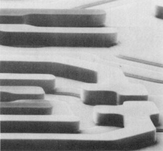
A cross-section showing multilevel connections
in a bipolar device. Fourteen separate layers are laid down
in the fabrication of interconnections such as that shown
here.
|
|
A challenge related to the problems of reactor design and engineering is the modeling and study of the fundamental chemistry occurring in manufacturing processes for semiconductors, optical fibers, magnetic media, and interconnection. For example, mathematical models originally developed for classic chemical engineering reactor systems such as continuously stirred tank reactors and plug-flow reactors are applicable to the reactors used for thin-film processing and can be modified to elucidate ways to improve these reactors. For these models to reach their full descrip- tive potential, detailed studies of the fundamental chemical reactions occurring on surfaces and in the gas phase are required. For example, etching rates, etching selectivity, line profiles, deposited film structure, film bonding, and film properties are determined by a host of variables, including the promotion of surface reactions by ion, electron, or photon bombardment. The fundamental chemistry of these surface reactions is poorly understood, and accurate rate expressions are particularly needed for electron-impact reactions (i.e., dissociation, ionization, and excitation), ion-ion reactions, neutral-neutral reactions, and ion-neutral reactions. The scale and scope of effort devoted in recent years to understanding catalytic processes need to be given to research on film deposition and plasma etching. Until we have a basic understanding of chemical reactions occurring at the surface and in the gas phase, it will be difficult to develop new etching systems. Research in this area has had a demonstrable impact on recent innovations in plasma processing. In the mid-1980's it was well known that a fluorine-containing plasma etches silicon at a rate significantly greater than the rate for silicon dioxide (SiO2), thus offering significant advantages for fabricating integrated circuits. However, well-controlled processes could not be developed that would perform in a production environment. The work of chemists and chemical engineers in elucidating the relevant chemical reactions and their kinetics was crucial to the identification of the important chemical species in the etching process and their reaction pathways. In addition, this work led to the discovery that the organic polymer photoresist contributed to plasma chemistry and selectivity in important ways. This in turn led to new, improved plasma processes that are currently being used in production. For magnetic media, mathematical models have enhanced our fundamental understanding of the manufacturing processes used to make uniform high-purity magnetic particles. Models for the kinetics and mechanisms of reactions and an improved understanding of the thermodynamics of producing inorganic salts are required. Modeling to describe the flows of viscous fluids has lead to better packaging of integrated circuits by assisting in the development of molding compounds and processes that provide for lower thermal shrinkage stresses, lower permeability, and lower thermal conductivity. Such modeling also contributes to the development of packaging materials and processes amenable to automation. |
|
Safety and environmental protection are extremely important concerns that present demanding intellectual challenges. The manufacture of materials and devices for information handling and storage involves substantial quantities of toxic, corrosive, or pyrophoric chemicals (e.g., hydrides and halides of arsenic, boron, phosphorus, and silicon; hydrocarbon and organic chlorides, some of which are suspected carcinogens; and inorganic acids). The expertise of chemical engineers in the safe handling and disposal of highly reactive materials is much needed in the electronics industry. Studies in California indicate that the semiconductor industry has an occupational illness rate three times that of general manufacturing industries. Nearly half of these illnesses involve systemic poisoning from exposure to toxic materials. Problems with groundwater contamination in Santa Clara County, California, have also raised concerns about how well the semiconductor industry is equipped to handle waste management and disposal. If the semiconductor and other advanced materials industries are to continue to prosper in the United States, it is important that the expertise of chemical engineers be applied to every aspest of chemical handling in manufacturing, from procurement through use to disposal. Also, it is essential that we explore other, novel manufacturing technologies that better utilitze the feedstock materials and produce smaller amounts of effluent that have to been disposed of. |